SENTECH Gesellschaft für Sensortechnik mbH

nano tech 2016

SENTECH develops, manufactures & globally sells innovative equipment focused on deposition, structuring & characterization of thin films in semiconductor technology, microsystems, photovoltaics, nanotechnology & materials research.
SENTECH provides innovative solutions for non-contact, non-invasive optical characterization using ellipsometry & reflectometry.
SENTECH is expert in etching & deposition of thin films by plasma process technology, further we offer ALD systems. The new SENTECH Metrology Application Lab at our Japanese distributor Hakuto will be opened in January 2016.

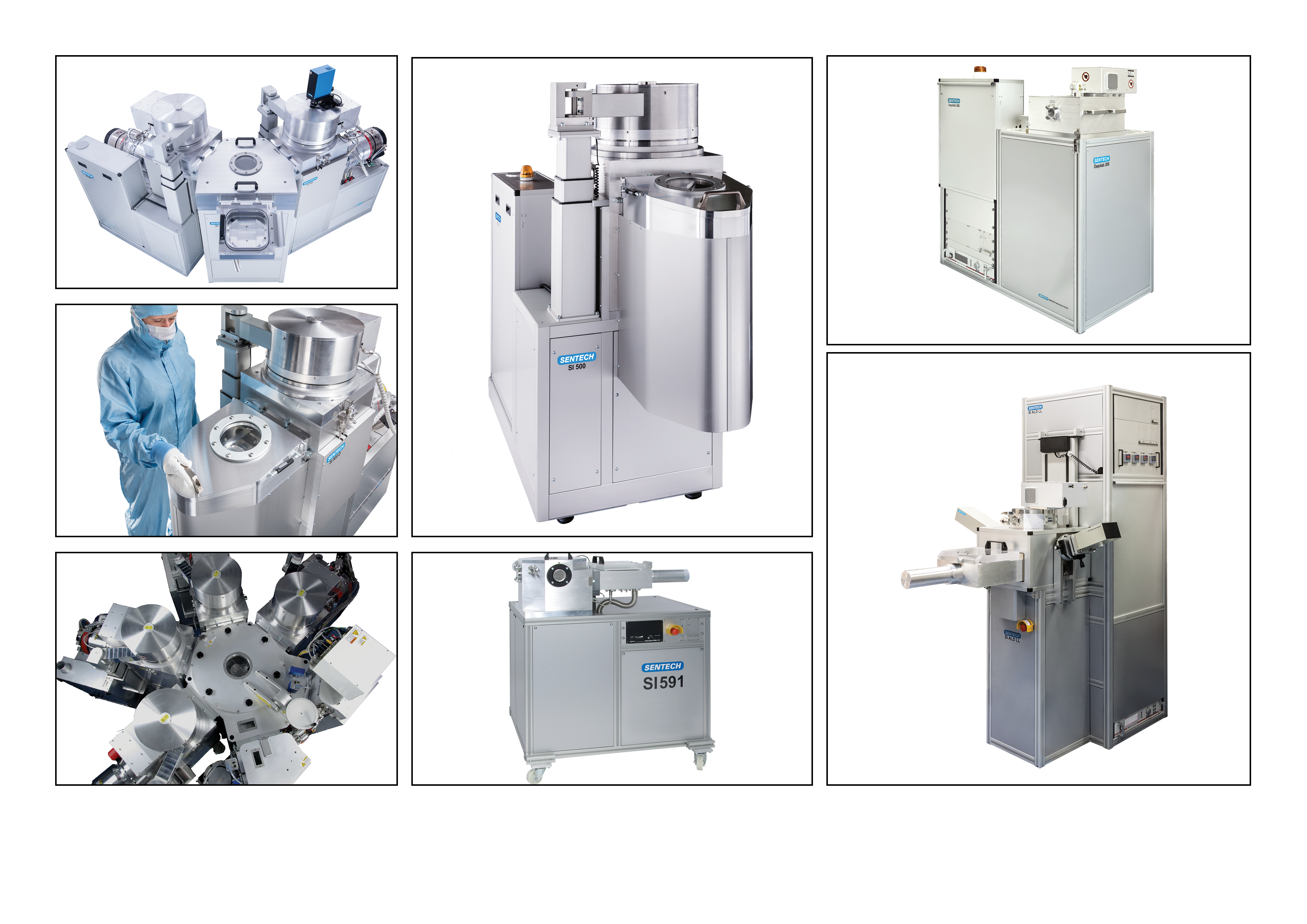
SENTECH sells equipment for plasma process technology (etching/coating equipment, ALD, ALE) and measuring equipment for optical thin film metrology (ellipsometers and reflectometers)

Products

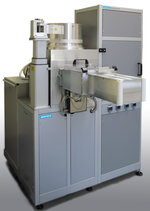
Plasma Process Technology:
ICP etching system for low damage etching, RIE etching system, ICPECVD system for low damage coating, ALD and ALE systems. All equipment can be integrated into one cluster.

Optical thin film metrology:
SENresearch 4.0 with wide spectral range from 190 - 3,500 nm, SENDIRA MIR spectroscopic ellipsometer, SENDURO MEMS an automated measurement platform, laser ellipsometer and others.

General Information

SENTECH Gesellschaft für Sensortechnik mbH
IVAM member
Konrad-Zuse-Bogen 13
82152 Krailling
Germany
Founding Year: 1987

Contact

Dr. Helmut Witek
+49 89 897 9607-0

Latest news

SENTECH SIPAR: Combining PEALD and PECVD in one Reactor
23.04.2018 SENTECHs new developed SIPAR allows combining PECVD and ALD in one reactor. With that a higher throughput and the combination …