IVAM Microtechnology Network
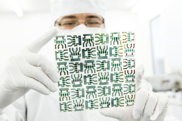
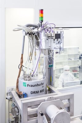
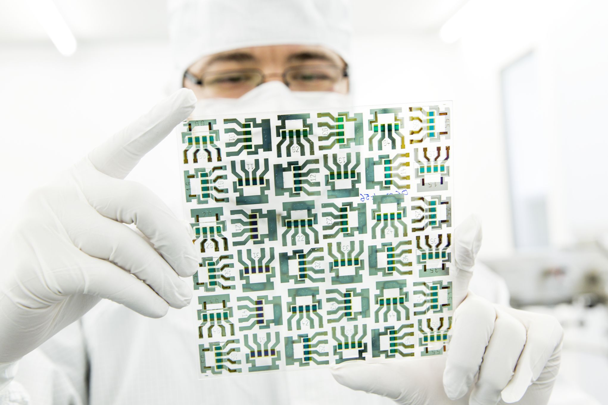
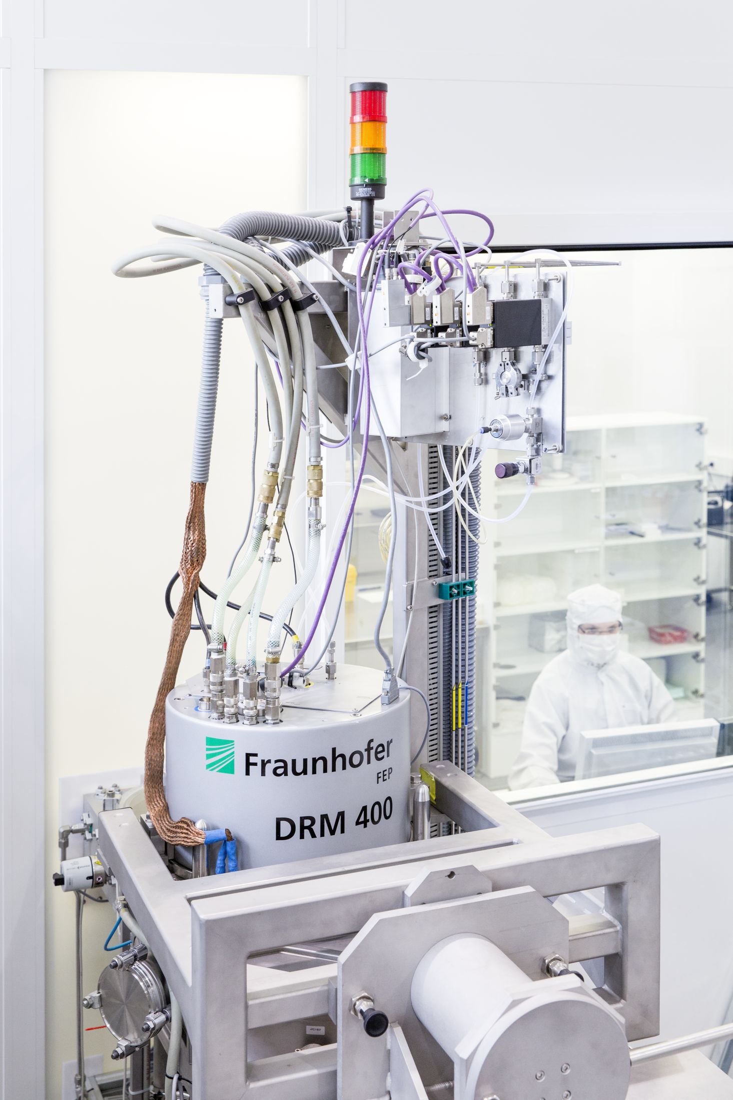
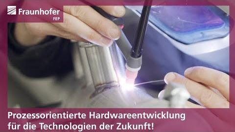
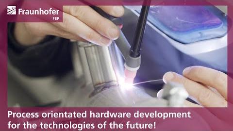
Fraunhofer Institute for Electron Beam and Plasma Technology FEP works on innovative solutions in the fields of vacuum coating and surface treatment. The core competences electron beam technology, plasma-assisted large-area and precision coating, roll-to-roll technologies and development of technological key components provide a basis for these activities.
Thus, Fraunhofer FEP offers a wide range of possibilities for research, development and pilot production, especially for the processing, sterilization, structuring and refining of surfaces as well as sensors and optical filters or for medical and biotechnological applications.
Our aim is to seize the innovation potential of the electron beam and plasma technologyfor new production processes and devices and to make it available for our customers.

 Präzisionsbeschichtung, Oberflächenbeschichtung, Elektronenstrahltechnik, Plasmatechnologie, Coating, surface technology, Energy Harvesting, Sensors, Precision, sputtering, Biomedizin, Oberflächentechnik, Plasma-Oberflächenbehandlung, Mikroelektronik, power-to-X, Sputterepitaxie