IVAM Microtechnology Network

As part of the European research project NanoHand the project partners KLOCKE NANOTECHNIK and TESCAN established a new SEM workbench installed as DemoLab in Aachen, Germany. The goal of NanoHand is to create the world’s first automated nanorobotics production system inside of a Scanning Electron Microscope (SEM), e.g. for producing carbon nanotube transistors. The SEM workbench is made out of a TESCAN high-resolution field emitter SEM (MIRA XM) and nanorobotics from KLOCKE NANOTECHNIK.
Plenty of new applications can be realized by this automated SEM workbench. A few typical examples are nano manipulation or 3D topography analysis in the fields of material and forensic research, micro tribology by friction analysis, stress tests, force-distance measurements on micro or nano components and systems, and semiconductor applications such as mask repair.
For the microtechnology sector the new DemoLab offers solutions beyond conventional methods: What’s the friction of a micropart moving in its system? How flexible is the microstructure in detail? What’s the surface roughness on the ground of a narrow micro channel? Are there any nano defects at the MEMS device?
Application-oriented demonstrations are possible after prior consultation. Furthermore the use of the system is provided as service, e.g. for nano manipulation, materials testing, friction measurement, 3D topography, roughness measurement, or micro/nano assembly.
KLOCKE NANTOECHNIK
Dr. Volker Klocke
info@nanomotor.de
www.nanomotor.de
 AEMtec.jpg)
AEMtec GmbH celebrates 25 years as a leading specialist in micro and optoelectronics. Marking the anniversary, the company is strengthening …
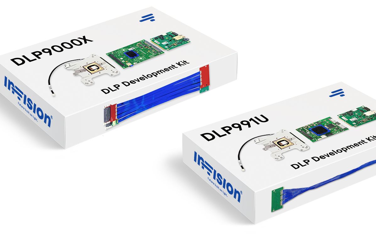
IN-VISION Technologies AG, an Austrian optics company and official Texas Instruments Design House Partner, is expanding access to its advanced …

Cubic’s Gasboard-2051 is an NDIR-based gas sensor solution designed for DLCO measurements, fully compliant with ERS/ATS standards. With high measurement …

 (4).png)